60-265 COMPUTER
SYSTEM ARCHITECTURE I: DIGITAL DESIGN
Solution for Midterm #2
Question: 1 (14
Marks)
An n-bit Binary
Counter using JK Flip-flops is to have the following facilities:
(i)
Parallel
Loading
(ii)
Synchronous
Clear.
It is required that
the Clear operation should over-ride both the operations of Parallel Loading
and Counting. The operation of Parallel Loading over-rides the operation of
Counting.
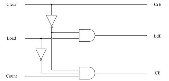
Draw the following schematic diagrams:
(a) The implementation for the control inputs for Synchronous
Clear, Parallel Loading and Counting so that the requirements for over-riding
can be met.
Solution:
|
Clear |
Parallel Load |
Count |
Operation |
|
1 |
X |
X |
Clear |
|
0 |
1 |
X |
Load |
|
0 |
0 |
1 |
Counting |
|
0 |
0 |
0 |
No operation |
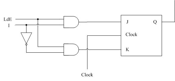
(b) A circuit, which implements the operation of parallel
loading on a JK FF.
Solution:
When LdE = 1, J = I and K = I’
So
if I = 1, J = 1 and K = 0 à Q = 1
If I = 0, J = 0 and K = 1 à Q = 0
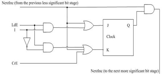
(c) The complete diagram of a typical stage of the counter.
Solution:
Question: 2 (12
Marks)
A
digital computer has a common bus system for 256 registers of 64 bits each.
(a) If the bus is
constructed through tri-state devices and a Decoder,
answer the following:
(i) What size of Decoder is needed?
Solution:
Decoder: 8-to-256 line Decider
(iii)
How many tri-state
devices
are required for the bus system?
Solution:
256X64 = 16384
(iv)
How many Control
inputs (of tri-state devices) will be connected to each output of the Decoder?
Hint: Each tri-state device has one control
input.
Solution:
64 control inputs, corresponding to 64 bits of a register will be
connected to each output of the decoder
(b) If the bus is
constructed with Multiplexers (MUXs), answer the following:
(i) What size of MUXs are needed?
Solution:
256-to-1 line MUX
(ii) How many selection inputs are
there in each MUX?
Solution:
Number of selection input = 8
(iii) How many MUXs are required for
the bus system?
Solution:
64 multiplexers
Question: 3 (18
Marks)
The
function table for a bi-directional m-bit Shift Register is as follows:
|
MODE CONTROL |
REGISTER OPERATIONS |
|
|
S1 |
S0 |
|
|
0 |
0 |
Shift
Left |
|
0 |
1 |
Parallel
Load |
|
1 |
0 |
No
Change |
|
1 |
1 |
Shift
Right |
Q.3 continued on the next page….
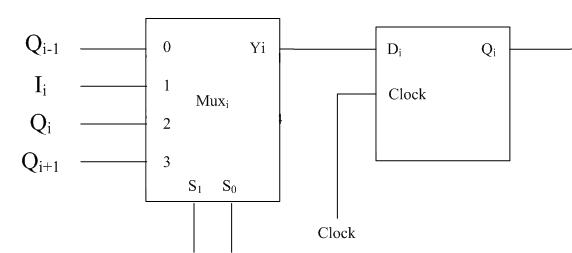
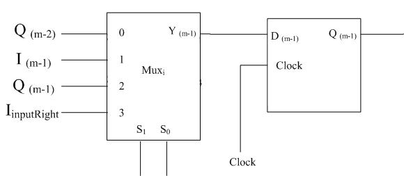
Question: 3 (….continued from the previous page) This Register is to be constructed by using the following
components:
§
D
flip-flops
§
4-to-1
multiplexers
§
Logic
gates, if required.
For this register,
draw the following:
(i)
a typical stage
Solution:
(ii)
two end-stages
Solution:
Least Significant Bit Stage
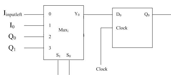
Most Significant Bit Stage of m-bit Shift Register
Question: 4 (a) (12
Marks)
State
the characteristic tables and excitation tables of the following flip-flops:
JK, T and D
Solution:
Characteristic Table
|
Jn |
Kn |
Qn+1 |
|
0 |
0 |
Qn |
|
0 |
1 |
0 |
|
1 |
0 |
1 |
|
1 |
1 |
Qn’ |
|
Tn |
Qn+1 |
|
0 |
Qn |
|
1 |
Qn’ |
|
Dn |
Qn+1 |
|
0 |
0 |
|
1 |
1 |
Excitation Table
|
Qn |
Qn+1 |
Jn |
Kn |
Tn |
Dn |
|
0 |
0 |
0 |
X |
0 |
0 |
|
0 |
1 |
1 |
X |
1 |
1 |
|
1 |
0 |
X |
1 |
1 |
0 |
|
1 |
1 |
X |
0 |
0 |
1 |
Question: 4 (b) (24 Marks)
It
is required to design a 3-bit counter, which can count up or count down,
depending upon a control input, X.
Obtain
its State Diagram.
Hint:
For X = 1, the counter may count as 0 à 1 à
2 à 3 à 4 à
5 à 6 à7 à
0.
For
X = 0, it may count as 0 à 7à
6 à 5 à 4 à
3 à 2 à1 à
0.
Solution:
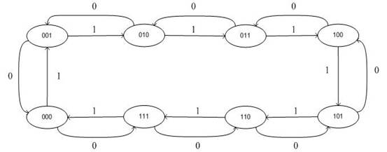
Use
the following three Flip-flops for the counter:
(i)
an
JK flip-flop in the Most Significant Bit position
(ii)
a
Delay flip-flop in the Least Significant Bit position
(iii)
a
Toggle flip-flop in the remaining Bit position.
Obtain the State Table for the counter.
Hint:
The State Table will have 11 columns and 16 rows as follows:
(i)
three columns of the
Present State (Q2, Q1, and Q0 ) and one column
of Control Input (X)
(ii)
three columns of the
Next State (Q2, Q1, and Q0 )
(iii)
four columns of inputs
for the three FFs namely J2, K2, T1 and D0.
Solution:
|
Present State |
|
NextState |
|
|||||||
|
Q2 |
Q1 |
Q0 |
X |
Q2 |
Q1 |
Q0 |
J2 |
K2 |
T1 |
D0 |
|
0 |
0 |
0 |
0 |
1 |
1 |
1 |
1 |
X |
1 |
1 |
|
0 |
0 |
0 |
1 |
0 |
0 |
1 |
0 |
X |
0 |
1 |
|
0 |
0 |
1 |
0 |
0 |
0 |
0 |
0 |
X |
0 |
0 |
|
0 |
0 |
1 |
1 |
0 |
1 |
0 |
0 |
X |
1 |
0 |
|
0 |
1 |
0 |
0 |
0 |
0 |
1 |
0 |
X |
1 |
1 |
|
0 |
1 |
0 |
1 |
0 |
1 |
1 |
0 |
X |
0 |
1 |
|
0 |
1 |
1 |
0 |
0 |
1 |
0 |
0 |
X |
0 |
0 |
|
0 |
1 |
1 |
1 |
1 |
0 |
0 |
1 |
X |
1 |
0 |
|
1 |
0 |
0 |
0 |
0 |
1 |
1 |
X |
1 |
1 |
1 |
|
1 |
0 |
0 |
1 |
1 |
0 |
1 |
X |
0 |
0 |
1 |
|
1 |
0 |
1 |
0 |
1 |
0 |
0 |
X |
0 |
0 |
0 |
|
1 |
0 |
1 |
1 |
1 |
1 |
0 |
X |
0 |
1 |
0 |
|
1 |
1 |
0 |
0 |
1 |
0 |
1 |
X |
0 |
1 |
1 |
|
1 |
1 |
0 |
1 |
1 |
1 |
1 |
X |
0 |
0 |
1 |
|
1 |
1 |
1 |
0 |
1 |
1 |
0 |
X |
0 |
0 |
0 |
|
1 |
1 |
1 |
1 |
0 |
0 |
0 |
X |
1 |
1 |
0 |
Question: 5 (20 Marks)
In
the schematic diagram of Figure 1, all the data inputs and data outputs of the
four registers (R0, R1, R2 and R3), and the multiplexer (MUX) are of n bits.
CONTROL
INPUTS: The two Selection inputs (S1 and S0) and the four
outputs (D0, D1, D2 and D3) of the
2-to-4-line Decoder are active high.
The
Selection input Sm of the MUX and the Load inputs of the four
registers (L0, L1, L2 and L3) are
also active high.
Are the following
register transfer operations feasible? For each of the feasible operations,
obtain the Boolean expression (in terms of S1, S0, Sm,
L0, L1, L2 and L3) for the
associated Condition.
Condition 1: R1ß R0, R2ß R0, R3ß R2
Condition 2: R0ß R3, R3ß R1, R2ß R3
Condition 3: R1ß R2, R2ß R0, R3ß R2
Solution:
Condition 1 is feasible.
Condition 1 = L0’.L1.L2.L3.S1’.S0’.Sm’
Condition 2 is feasible.
Condition 2 = L0.L1’.L2.L3.S1.S0.Sm
Condition 3 is infeasible.
The outputs of both R2 and R0
cannot simultaneously be loaded into the bus.
* * * * * * * * * *