Saturday,
27th June 2009
Intersession 2009 Time: 3.30 pm to 6.30 pm
COMPUTER SYSTEM ARCHITECTURE I: Digital Design
|
Student’s
Name: |
|
|
Student’s
Number: |
Seat
Number: |
Question: 1 (a) (5
Marks)
(i) Prove the following identity:
(X + Y).(X + Y’) = X
(ii) If
F1
= (A + B’ + C + D).(A’ + B’
+ C + D).( A’ + B’ + C + D’).(A + B + C + D’).(A’ + B + C + D’),
and if
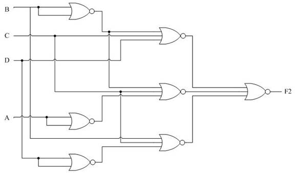
F2 = (B’
+ C + D).( A’ + B’ + C).( B + C + D’),
use Boolean algebra to prove that:
F1 = F2 .
(iii)
Implement the function F2 by
using NOR gates only.
Solution:
Question1(a1)
(X + Y).(X + Y’)
= X + X.Y’ + X.Y
= X(1 + Y’ + Y) = X
Question1(a2)
F1
= (A + B’ + C + D).(A’ + B’ + C + D).( A’ + B’ + C + D’).(A + B + C + D’).(A’ + B + C + D’)
= (A + B’ + C + D).(A’ + B’ + C + D). (A’ + B’ + C + D). (A’ + B’ + C + D’). (A + B + C + D’). (A’ + B + C + D’)
------------By using X.X = X
=(B’ + C + D).(A’ + B’ + C).(B + C + D’)
----------By using (X+ Y).(X + Y’) = X
=F2
Question1(a3)
F2’’ = ((B’ + C + D).(A’ + B’ + C).(B + C + D’))’’
=((B’ + C + D)’ + (A’ + B’ + C)’ + (B + C + D’)’)’
Question: 1 (b) (5
Marks)
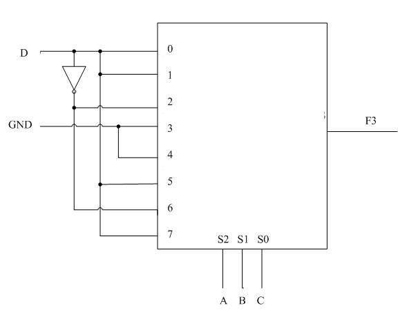
Use
a 8-to-1 MUX, along with an Inverter, to obtain an implementation for the
following function:
F3(A, B, C, D) = Σ ( m(1, 3,
4, 11, 12, 15).
Solution:
F3 = A’.B’.C’.D + A’.B’.C.D + A’.B.C’.D’ + A.B’.C.D + A.B.C’.D’ + A.B.C.D
Y = A’.B’.C’.D0 + A’.B’.C.D1 +
A’.B.C’.D2 + A’.B.C.D3 + A.B’.C’.D4 + A.B’.C.D5
+ A.B.C’.D6 + A.B.C.D7
On comparing
D = D0 = D1 = D5 =D7
D’ = D2 = D6
0 = D3 = D4
Question: 1 (c) (5
Marks)
Use
an Active Low 4-to-16 line Decoder, along with two gates to obtain an implementation for the following two functions:
(i)
F4(A,
B, C, D) = Σ ( m(1, 6, 8, 11, 13, 15)
(ii)
F5(A,
B, C, D) = Σ ( m(0, 3, 4, 6, 7, 9, 11, 12, 13, 14, 15).
For
implementing each of the two functions F4(A, B, C, D) and F5(A,
B, C, D), choose a gate with as small
a value of fan-in as possible.
Solution:
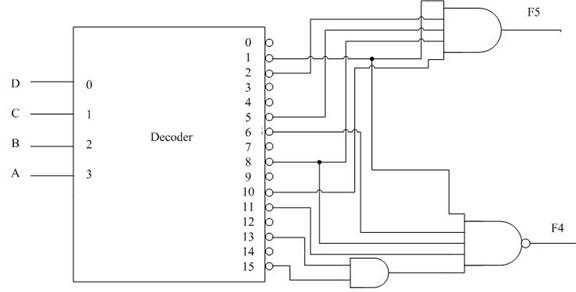
Example: Y6 = (A’.B.C.D’)’ = A + B’ + C’ + D
F4 = Σ m(1,6,8,11,13,15)
= ((A’.B’.C’.D) + (A’.B.C.D’) + (A.B’.C’.D’) + (A.B’.C.D) + (A.B.C’.D) + (A.B.C.D))’’
= ((A’.B’.C’.D)’.(A’.B.C.D’)’.(A.B’.C’.D’)’.(A.B’.C.D)’.(A.B.C’.D)’.(A.B.C.D))’’
= (Y1.Y6.Y8.Y11.Y13.Y15)
F5 = Σ m(0,3,4,6,7,9,11,12,13,14,15)
= Π M(1,2,5,8,10)
= Y1.Y2.Y5.Y8.Y10
Question: 2 (10
Marks)
Two
Boolean functions are given as:
F6(A, B, C, D) = ΠM(2, 3, 6, 7, 9, 10, 13, 15);
F7(A, B, C, D) = ΠM(1, 2, 3, 5, 9, 10, 11, 12).
F8
is obtained as follows:
F8(A,
B, C, D) = (F6(A, B, C, D) F7(A,
B, C, D)).
(i)
Express
F8(A, B, C, D) in the following format:
F8(A, B, C, D) = Σm( ).
Solution:
F8 = Σ m(1,5,6,7,11,12,13,15)
Q.2 continued on the next page….
Question: 2
(….continued from
the previous page)
(ii)
Draw
the Karnaugh map for the following function
F9(A, B, C, D) = Σ( m( 1, 5, 6, 7, 11, 12, 13, 15).
(iii)
Obtain
all the Prime Implicants for F9(A,
B, C, D).
Which of the Prime Implicants of F9(A, B, C, D) are
Essential?
(iv) Use Karnaugh map to obtain the simplified expression in the SOP
form for the function F9(A,
B, C, D).
Solution:
(ii)
|
K-MAP |
CD |
||||
|
AB |
|
00 |
01 |
11 |
10 |
|
00 |
0 |
1 |
0 |
0 |
|
|
01 |
0 |
1 |
1 |
1 |
|
|
11 |
1 |
1 |
1 |
0 |
|
|
10 |
0 |
0 |
1 |
0 |
|
(iii)
Prime Implicants
A.B.C’, A’.C’.D, A’.B.C, A.C.D, B.D
Essential Prime Implicants
A.B.C’, A’.C’.D, A’.B.C, A.C.D
(iv)
F9 = A.B.C’ + A’.C’.D + A’.B.C + A.C.D
Question: 3 (a) (6
Marks)
State
the characteristic tables and excitation tables of the following flip-flops:
T, D and SR
Solution:
Characteristic Table
SR
|
Sn |
Rn |
Qn+1 |
|
0 |
0 |
Qn |
|
0 |
1 |
0 |
|
1 |
0 |
1 |
|
1 |
1 |
Invalid |
Toggle
|
Tn |
Qn+1 |
|
0 |
Qn |
|
1 |
Qn’ |
Delay
|
Dn |
Qn+1 |
|
0 |
0 |
|
1 |
1 |
Excitation Table
|
Qn |
Qn+1 |
Tn |
Dn |
Sn |
Rn |
|
0 |
0 |
0 |
0 |
0 |
X |
|
0 |
1 |
1 |
1 |
1 |
0 |
|
1 |
0 |
1 |
0 |
0 |
1 |
|
1 |
1 |
0 |
1 |
X |
0 |
Question: 3 (b) (9
Marks)
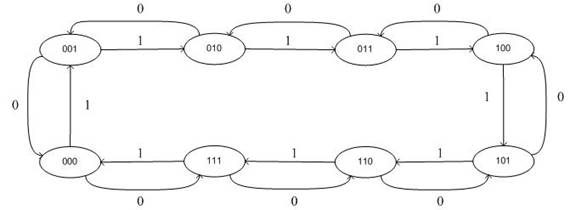
A
3-bit counter can count up or count
down, depending upon a control input, X. It
counts up when X = 1as follows:
0 à
1 à 2 à 3 à
4 à 5 à 6 à7
à 0.
When X = 0, it goes through
the following sequence of states:
0 à 7à
6 à 5 à 4 à
3 à 2 à1 à
0.
Obtain
its State Diagram.
Use
the following three Flip-flops for the counter:
(i)
an
Toggle flip-flop in the Most Significant Bit position
(ii)
an
SR flip-flop in the Least Significant Bit position
(iii)
a
Delay flip-flop in the remaining Bit position.
Obtain the State Table for the counter.
Draw the K-map for the Delay flip-flop only.
Read from the K-map the simplified expression for the D input of the FF in SOP
format.
Solution:
State Diagram
State Table
|
|
|
NextState |
|
|||||||
|
Q2 |
Q1 |
Q0 |
X |
Q2 |
Q1 |
Q0 |
T2 |
D1 |
S0 |
R0 |
|
0 |
0 |
0 |
0 |
1 |
1 |
1 |
1 |
1 |
1 |
0 |
|
0 |
0 |
0 |
1 |
0 |
0 |
1 |
0 |
0 |
1 |
0 |
|
0 |
0 |
1 |
0 |
0 |
0 |
0 |
0 |
0 |
0 |
1 |
|
0 |
0 |
1 |
1 |
0 |
1 |
0 |
0 |
1 |
0 |
1 |
|
0 |
1 |
0 |
0 |
0 |
0 |
1 |
0 |
0 |
1 |
0 |
|
0 |
1 |
0 |
1 |
0 |
1 |
1 |
0 |
1 |
1 |
0 |
|
0 |
1 |
1 |
0 |
0 |
1 |
0 |
0 |
1 |
0 |
1 |
|
0 |
1 |
1 |
1 |
1 |
0 |
0 |
1 |
0 |
0 |
1 |
|
1 |
0 |
0 |
0 |
0 |
1 |
1 |
1 |
1 |
1 |
0 |
|
1 |
0 |
0 |
1 |
1 |
0 |
1 |
0 |
0 |
1 |
0 |
|
1 |
0 |
1 |
0 |
1 |
0 |
0 |
0 |
0 |
0 |
1 |
|
1 |
0 |
1 |
1 |
1 |
1 |
0 |
0 |
1 |
0 |
1 |
|
1 |
1 |
0 |
0 |
1 |
0 |
1 |
0 |
0 |
1 |
0 |
|
1 |
1 |
0 |
1 |
1 |
1 |
1 |
0 |
1 |
1 |
0 |
|
1 |
1 |
1 |
0 |
1 |
1 |
0 |
0 |
1 |
0 |
1 |
|
1 |
1 |
1 |
1 |
0 |
0 |
0 |
1 |
0 |
0 |
1 |
|
K-MAP |
Q0X |
||||
|
Q2Q1 |
|
00 |
01 |
11 |
10 |
|
00 |
1 |
0 |
1 |
0 |
|
|
01 |
0 |
1 |
0 |
1 |
|
|
11 |
0 |
1 |
0 |
1 |
|
|
10 |
1 |
0 |
1 |
0 |
|
D1 = Q1’.Q0’.X’ + Q1.Q0’.X + Q1’.Q0.X + Q1.Q0.X’
Question 4 (10 marks)
A
4-bit bi-directional shift register is designed to have the following 4
operations:
(i)
No Change
(ii)
Shift Right
(iii) Shift Left
(iv)
Parallel Load
The
shift register is enclosed in an IC package.
(a) Draw the block
diagram of the IC, showing all inputs and outputs. State its Function Table.
Solution:
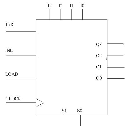
|
S1 |
S0 |
Operation |
|
0 |
0 |
No Change |
|
0 |
1 |
SR |
|
1 |
0 |
SL |
|
1 |
1 |
Parallel Load |
(b)
Draw
the block diagram, using two ICs of (a) above, to produce an 8-bit
bi-directional shift register, having the 4 operations described above.
Solution:
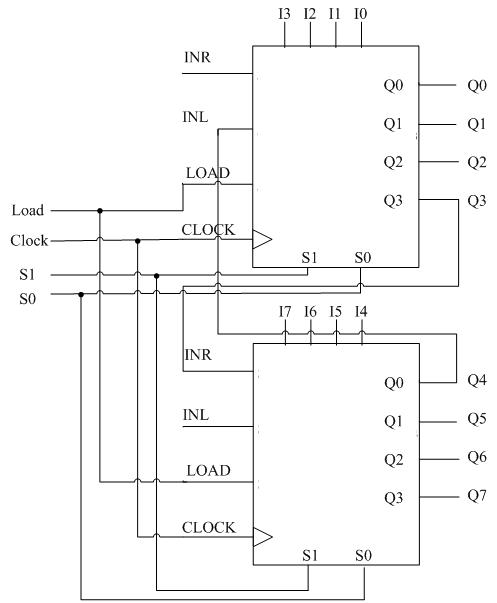
(c)
The
content of an 8-bit bi-directional shift register is initially
1010 1110.
The Shift Right operation is performed on the
register, three times, with an input of 101.
This
is followed by a Shift Left operation, two times, with an input of 00.
Show the contents of the register
after each shift.
Solution:
10101110
11010111
01101011
10110101
01101010
11010100
Question: 5 (10
Marks)
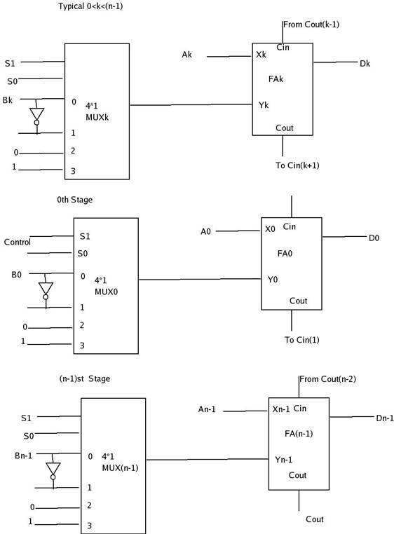
An Arithmetic Circuit is to be constructed
for the following operations on two n-bit numbers A and B:
(i) A +
B
(ii) A +
B + 1
(iii) A –
B – 1
(iv) A –
B
(v) A
(vi) A +
1
(vii)
A - 1
The Arithmetic Circuit should use 4-to-1 line
multiplexers, I-bit Full Adders and Inverters.
For
this Arithmetic Circuit, draw the following stages:
a) a typical stage
b) the 0th stage
c) the (n-1)st stage.
Solution
a)
Function Table
|
S1 |
S0 |
Cin |
Function |
|
0 |
0 |
0 |
A+B |
|
0 |
0 |
1 |
A+B+1 |
|
0 |
1 |
0 |
A-B-1 or A+B’ |
|
0 |
1 |
1 |
A-B |
|
1 |
0 |
0 |
A |
|
1 |
0 |
1 |
A+1 |
|
1 |
1 |
0 |
A-1 |
|
1 |
1 |
1 |
A |
Question 6 (10 marks)
The
Adder-Logic Unit of a 16-bit computer has three sources of data input:
a 16-bit Accumulator (AC), a 16-bit Data
Register (DR) and an 8-bit Input Register (
Its
output is to be stored in AC. (Refer to the Basic Computer of Fig 1.)
The
Adder-Logic Unit (ALU) is designed for performing the following operations:
(i)
ANDing
of variables stored in AC and DR,
(ii)
Addition
of variables stored in AC and DR,
(iii) Transfer from DR to AC,
(iv) Transfer from INPR to
AC(0-7),
(v) Complement of the
variable stored in AC,
(vi) Shifting Right the
variable stored in AC,
(vii)Shifting Left the variable stored in AC.
Assume
that for each of the above 7 operations, a distinct control input is available.
Only when a control input is 1, that the associated operation is to be
performed.
The
ALU has 16 stages,
from i = 0 (the least significant bit stage) to
i = 15 (the most
significant bit stage).
Besides
the 7 control inputs for each of the
7 operations, there is another control
input for Loading the JK Flip-flops.
a) Use a JK Flip-flop, a Full Adder and logic gates to draw the stage for i = 3.
The inputs to each stage are DR(i), AC(i),
AC(i + 1) and AC(i - 1). The Full Adder in the i-th stage of the
b) Explain the differences between the stage for i = 3 and
each of the two end-stages.
Solution:
a)
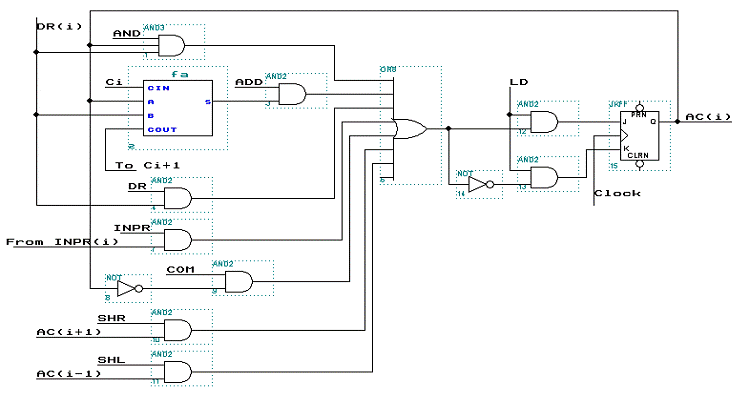
CONTROL INPUTS:
LD, AND,
ADD, DR, INPR, COM, SHR and SHL
OTHER INPUTS:
DR(i),
INPR(i), AC(i), AC(i+1), AC(i-1),
Carry Input Cin from the previous stage.
OUTPUTS:
AC(i) and
Carry Output which goes to the carry input of the next stage.
b) In stage 0, there
will be no Carry Input (Ci) from the previous stage. Instead, Ci will become a control input.
In stage i = 15, there will be no Carry
Output Ci+1 to the next stage.
Instead, Cout will be loaded to the flip-flop E.
In stage i = 15, there will be no AND gate
with INPR and INPR(i) as the inputs.
The OR gate, which feeds the data input for
loading into the JK flip-flop will have a fan-in of 6 (in stage i = 3 the fan-in
of this or gate is 7).
Question 7 (10 marks)
(a) Use Table
1 to obtain the logical expression for the Write input for memory.
Solution:
WRITE = RT1 +
D3T4 + D5T4 + D6T6
(b) Refer to Table 1
and Figure 1. S0, S1
and S2 are the control inputs for the 16-bit common bus. Obtain the Boolean expression for S1
in terms of the following variables:
(i) 8 Boolean variables: D0 to D7
(ii) 16 Boolean variables T0 to T15
(iii)
12 bits B0 to B11
(iv)
Boolean variables R and I
Solution:
S1
= x7 + x2 + x3 + x6
x2
is for loading PC onto the bus.
x2
= R’T0 + R0T0 + D5T4
= (R’ + R)T0 + D5T4
= T0 + D5T4
x3
is for loading DR onto the bus.
x3
= D6T6
x6
is for loading TR onto the bus.
x6
= RT1
x7
is for loading from memory onto the bus (i.e., for
x7
= R’T1 + D7’IT3 + (D0 + D1
+ D2 + D6)T4
S1
= T0 + D5T4 + D6T6 + RT1
+ R’T1 + D7’IT3 + (D0 + D1
+ D2 + D6)T4
= T0 + T1 + (D0
+ D1 + D2 + D6)T4 + D7’IT3
+ D6T6
Question 8 (20 marks)
Refer to Table 1
and Figure 1. At the beginning of
an instruction cycle, the contents of two of the registers, two of the
flip-flops and some of the memory locations in the basic computer are given
below. All values are in hexadecimal.
|
Register/Flip-flop/Memory Location |
Contents |
|
PC |
2A2 |
|
AC |
A35F |
|
R |
0 |
|
IEN |
1 |
|
2A2 |
C000 |
|
000 |
0446 |
|
446 |
1F03 |
|
F03 |
2A45 |
Starting with the above initial values at T0,
the following steps are taken in sequence:
Step 1: First the memory instruction at address 2A2
is executed.
Step 2: After executing Step 1, the memory
instruction at address 446 is executed.
During execution of the two steps, for each
clock cycle, starting from T0 for each of the steps, work out the following:
(i)
Specify the register
transfer operation(s) being executed during the clock cycle.
(ii)
For
Step 1, answer the following:
a.
What
is the value of I immediately after the clock cycle T2 is over?
b.
Which
instruction is being executed during the Step?
(iii)
For
Step 2, answer the following:
a.
What
is the value of I immediately after the clock cycle T2 is over?
b.
Which
instruction is being executed during the Step?
c.
What
is the value of E immediately after the clock cycle T5 is over?
(iv)
Specify the contents
(in hexadecimal) of registers PC, AR, DR, AC and IR at the end of each clock
cycle.
If the contents of a register are not yet known, specify it as X.
Please see page 5 for Figure 1.
Please see page 6 for Table
1.
NOTE: Figure 1 is Fig 5-4
of the text book. Table 1 is Table 5-6 of the text book.
Solution:
(i) and (iv)
|
|
i |
PC |
AR |
IR |
DR |
AC |
|
T0 |
AR ← PC |
2A2 |
2A2 |
X |
X |
A35F |
|
T1 |
IR ← M[AR] |
2A3 |
2A2 |
C000 |
X |
A35F |
|
|
PC ← PC + 1 |
|
|
|
|
|
|
T2 |
AR ← IR(11-0) |
2A3 |
000 |
C000 |
X |
A35F |
|
|
I ← IR(15) |
|
|
|
|
|
|
|
D0…D7 ← Decode IR(17-14) |
|
|
|
|
|
|
T3 |
AR ← M[AR] |
2A3 |
446 |
C000 |
X |
A35F |
|
T4 |
PC ← AR |
446 |
446 |
C000 |
X |
A35F |
|
|
SC ← 0 |
|
|
|
|
|
|
T0 |
AR ← PC |
446 |
446 |
C000 |
X |
A35F |
|
T1 |
IR ← M[AR] |
447 |
446 |
1F03 |
X |
A35F |
|
|
PC ← PC + 1 |
|
|
|
|
|
|
T2 |
AR ← IR(11-0) |
447 |
F03 |
1F03 |
X |
A35F |
|
|
I ← IR(15) |
|
|
|
|
|
|
|
D0…D7 ← Decode IR(17-14) |
|
|
|
|
|
|
T3 |
(No action) |
447 |
F03 |
1F03 |
X |
A35F |
|
T4 |
DR ← M[AR] |
447 |
F03 |
1F03 |
2A45 |
A35F |
|
T5 |
AC ← AC + DR |
447 |
F03 |
1F03 |
2A45 |
CDA4 |
|
|
E ← Cout |
|
|
|
|
|
|
|
SC ← 0 |
|
|
|
|
|
(ii) (a)
I = 1 (b) BUN
(iii) (a) I = 0 (b) ADD (c) E = 0